제품소개
해외 우수한 분석, 측정, 계측기기 제조회사의 독점 대리점 !


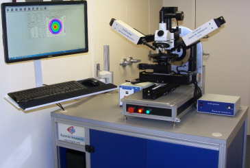
박막두께측정기
SE SeriesSE200BA-MSP300
BEST Good
제품구성
| SE200BA-MSP300 | |
|---|---|
| Detector | Detector Array |
| Light Source | High Power DUV-Vis-NIR Combined Light Source for SE and High Power Visible Light Source for MSP |
| Incident Angle Change | Automatic with Program setting |
| Stage | Automatic Mapping with Rho-Theta configuration |
| Software | |
| Computer & Monitor | Intel Duo Core Processor, 19" Wide Screen LCD |
| Power | 110 - 240 VAC /50-60Hz, 6 A |
제품사양
| SE200BA-MSP300 | |
|---|---|
| Wavelength range | 250 to 1000 nm for SE and 400 to 850 nm for MSP |
| Ellipsometer Wavelength resolution | ~ 1 nm |
| Spot Size | 1 to 5 mm variable for SE |
| Incident Angle Range | 10 to 90 degree |
| Incident Angle Change Resolution | 0.01 degree |
| Digital Imaging | 1.3 MegPixels |
| Effective Magnification | 1200x |
| MSP Beam Size | Adjustable 10 - 500 μm |
| Sample Size | Up to 300 mm in diameter |
| Substrate Size | Up to 20 mm thick |
| Measurable thickness range | 0 nm to 10 μm |
| Measurement Time | ~ 1s/Site |
| Accuracy | Better than 0.25% |
| Repeatability | < 1 Å (1 sigma from 50 thickness readings for 1500 Å Thermal SiO2 on Si Wafer) |
옵션
| SE200BA-MSP300 |
|---|
|
|
| High resolution digital camera |
Ultra Long work distance objective for MSP |
|
| Heating /Cooling Stage |
| Vertical Sample Mounting Goniometer |
| Wavelength extension to further DUV or IR range |
| Scanning Monochromator Setup |
적용분야
| SE200BA-MSP300 |
|---|
|
|
| Forensics, Biological films and materials |
Inks, Mineralogy, Pigments, Toners |
| Optical coatings, TiO2, SiO2, Ta2O5..... |
| Semiconductor compounds |
| Functional films in MEMS/MOEMS |
| Amorphous, nano and crystalline Si |