제품소개
해외 우수한 분석, 측정, 계측기기 제조회사의 독점 대리점 !


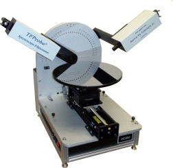
박막두께측정기
SE SeriesSE300BM
BEST Good
제품구성
| SE300BM | |
|---|---|
| Detector | Detector Array |
| Light Source | Adjustable intensity Vis-NIR Light Source |
| Incident Angle Change | Manual |
| Stage | Black Anodized Alumnium Sample holder for up to 200 mm or 150 x 150 mm samples |
| Software | |
| Computer & Monitor | Intel Duo Core 2.0 GHz, 19" Wide Screen LCD |
| Power | 110 - 240 VAC /50-60Hz, 6 A |
제품사양
| SE300BM | |
|---|---|
| Wavelength range | 400 to 1100 nm |
| Wavelength resolution | ~ 1 nm |
| Spot Size | 1 to 5 mm variable |
| Incident Angle Range | 0 to 90 degree |
| Incident Angle Change Resolution | 5 degree interval |
| Sample Size | Up to 200 mm in diameter or 150 mm square |
| Substrate Size | Up to 20 mm thick |
| Measurable thickness range | 5 nm to 30 μm |
| Measurement Time | ~ 1s/Site |
| Accuracy | Better than 0.25% |
| Repeatability | < 1 Å (1 sigma from 50 thickness readings for 1500 Å Thermal SiO2 on Si Wafer) |
옵션
| SE300BM |
|---|
|
|
| Automatic Goniometer for Incident angle changes |
| Mapping Stage (X-Y mode or Rho-Theta mode) |
| Heating /Cooling Stage |
| Vertical Sample Mounting Goniometer |
|
|
| Combined with Microspectrophotometer (MSP) for patterned sample measurement with digital imaging functions |
적용분야
| SE300BM |
|---|
|
|
| Forensics, Biological films and materials |
Inks, Mineralogy, Pigments, Toners |
| Optical coatings, TiO2, SiO2, Ta2O5..... |
| Semiconductor compounds |
| Functional films in MEMS/MOEMS |
| Amorphous, nano and crystalline Si |
| Various TCO films (ITO, FTO, IZO, AZO...) |