제품소개
해외 우수한 분석, 측정, 계측기기 제조회사의 독점 대리점 !


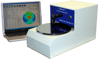
박막두께측정기
Mapping SystemSRM300
BEST Good
제품구성
| SRM300 | |
|---|---|
| Detector | CCD Array with 2048 pixels |
| Light Source | DC regulated Tungsten-Halogen |
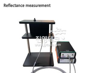
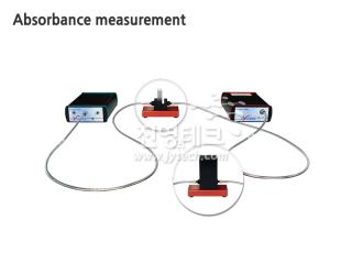
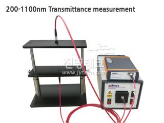
| Light Delivery | Optics |
| Stage | Black Anodized Aluminum Alloy Vacuum chuck holds 300 mm wafer |
| Communication | USB |
| Measurement Type | Film thickness, reflection spectrum, refractive index |
| Software | TFProbe 2.X/3.X |
| Computer | Intel Core 2 Duo Processor with 300GB Hard drive and DVD+RW Burner plus 20” LCD Monitor |
| Power | 110 - 240 VAC /50-60Hz, 3 A |
제품사양
| SRM300 | |
|---|---|
| Wavelength range | 400 to 1050 nm |
| Spot Size | 500 μm to 5 mm |
| Sample Size | 300 mm in diameter |
| Substrate Size | Up to 50 mm thick |
| Measurable thickness range | 50 nm to 50 μm |
| Measurement Time | 2ms - 1s /site typical |
| Accuracy | Better than 0.5% (comparing with ellipsometry results for Thermal Oxide sampleby using the same optical constants) |
| Repeatability | <2Å (1 sigma from 50 thickness readings at center for 1500 Å Thermal SiO2 on Si Wafer) |
옵션
| SRM300 |
|---|
|
|
| Large Spot Accessories for featured structure measurement |
Small spot accessories for highly non uniform samples |
| Other Sample Size: 200mm wafer (SRM300-200) |
적용분야
| SRM300 |
|---|
|
|
| Biological films and materials |
Optical coatings, TiO2, SiO2, Ta2O5..... |
| Semiconductor compounds |
| Functional films in MEMS/MOEMS |
Amorphous, nano and crystalline Si |
적용사례
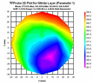
| 2D thicknesses plot for Nitride layer in a three layer stack (Nitride-Oxide-Nitride on Glass) | |
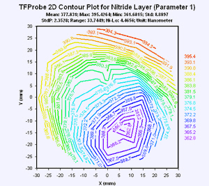
| |
| 2D contour plot for Nitride layer in a three layer stack (Nitride-Oxide-Nitride on Glass) | |
| |